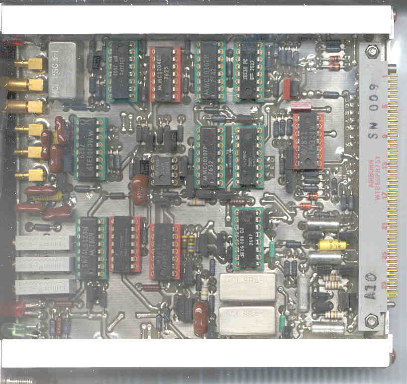
MCL PSC 3-1, 10131, MC12040P, MCIOI02P, F IO116 PC
MC10131p, LM308N, MC10107p, F 10125pc, LM324N
SN74LS123N, F 74ls32PC, lm324n, dg 508 cj,
mcl sra-1, mcl sra-1
2 Xtals in series at J11 & J12
A-10 FREQ. MULTI. 100-102727
N M EFC MAN EXT J12 J11 J10 J9 J8 J7 A
G R P P P C C C C C C R
r e o o o o o o o o o e
n d t t t n n n n n n d
MCL PSC 3-1, 10131, MC12040P, MCIOI02P, F IO116 PC
MC10131p, LM308N, MC10107p, F 10125pc, LM324N
SN74LS123N, F 74ls32PC, lm324n, dg 508 cj,
mcl sra-1, mcl sra-1
2 Xtals in series at J11 & J12