PIC 16F88
Getting Started
© Brooke Clarke 2006
Background
I/O pin count
Special Feature Pin Assignment
Program Memory Size
Packages & Programming
Choosing the Language for writing PIC Code
Printed Page Formatting
Tables (Computed Goto)
OSCCAL
Precision Interrupt Timing
App Notes
In Circuit Debugging
Debugging without ICD
LCD Interface
Links
Code Generators
General
Linkers & Loaders
Background
It used to be that the 16F84 was an optimal unit for
general hobby use. But as of June 2006 the 16F88 looks to be a
better choice for a number of reasons.
3 Feb 2007 - I'm starting to think the skinny (0.300") 28 pin PICs may
be more useful than the 16F88. There are a bunch of these.
The 16F876A or 16F916 (a nano watt 876A). Note that these are
SKINNY (0.3") so when they are on a proto board there are still 4 holes
for each pin. That's not the case with the more common 0.6" 28
pin ICs.
11 April 2007 - The 28 pin DIP package is 1/2" longer than the 18 pin
16F88 DIP package and that hurts when you're getting a PCB made, like
those from
ExpressPCB. So the I still like the 16F88 or the 16F87x or 16F88x which have more memory, but keep the 18 pin count footprint.
There is another reason that 18 pins is optimal, it's the minimum
number supported by ICD2, so the smaller pin count parts need an
optional headder to work with ICD2. That's too bad since the PIC
Kit 2 is a great product. Even though at one time I had a
discount cupon for one I never got it.
11 Apr 07 - But today I would recommend the PICkit 2 since the nanowatt
type PICs have more useable pins (see below). If you have zero
experience it would be an economical way to get started. The
Microchip Getting Started with PIC® Microcontrollers web page has links to the
PICkit2 Getting Started page. There's now a
PICkit™ 2 Debug Express
to go with the PICkit2 (I'm going to look into this, may get
them). Note the PICket2 supports all the 8, 14 and 20 pin PICs (I
think the 20 pin PICs are extensions on the 14 pin parts, and are not
more powerful than the 18 pin parts) but not the more powerful 18 pin
parts like the 16F84 or 16F88.
This web page is aimed at those who are not at zero.
Nano Watt Feature Set
This feature set includes an internal
oscillator that does not use any I/O pins and typically the 2 pins that
were for the oscillator are now I/O pins. Also there's the
ability to detect primary oscillator failure and switch to a secondary
oscillator (very handy for my clocks). This is very desirable
both for the oscillator and more useable I/O pins.
The Product Slection Guide has pages "Pin Count Compatibility Chart"
showing each PIC outline and under that a list of all the model numbers
that match the outline. In the 00148M.pdf file there are 50 model
numbers listed for the 28 pin package. Note the outline includes
lables on all the pins so all the models listed are interchangable to
some extent.
I/O pin count
Microchip doesn't really tell it like it is. Many of the
PICs let you use the /MCLR (say "not master clear" or "not" "M" "C" "L"
"R") pin as an input only pin. But then this pin is NOT an I/O
(say "I" "O" or "Input Output") pin but rather just an I (Input)
pin. The data sheets typically count this pin as an I/O
pin. The Data Sheet (DS_30487c.pdf) for the 16F88 does not
mention the number of I/O pins on page 3 but instead shows the pin out
diagram where pin 4 is labeled as "RA5/MCLR/VPP", the implication is
that you get a full I/O with RA5 but that's not the case. An
experienced (someone who has suffered and learned) PIC person knows
this, but if you're a newbie you need to keep it in mind. You can
not use the 16F88 RA5 pin for Output!
The 18 pin 16F88 has 2 pins for the power and ground. leaving 16 pins
that can be assigned many ways. The maximum I/O count is 8 pins
for Port B and 7 I/O pins for Port A and an Input only pin on RA5 for a
total of 15.5 I/O pins.
But this is also dependent on how you program the chip.
- If you
use the Picstart Plus then you get the full 15.5 I/O pins.
- If the
ICD 2 (In Circuit Debugger version 2) is used for either programming or
debugging then you need to leave /MCLR (RA5) with a 10 k resistor to
+5, so you loose the Input Only pin as an Input leaving you with 15 I/O
pins (you can get this pin back if you use it with a switch where the
10 k resistor is it's pullup). Although you can share the
clock and data pins, there's a number of conditions that must be
met. So I leave these alone if at all possible to avoid the
hassle.
- If you enable Low-Voltage ICSP (In Circuit Serial
Programming) (+5 V only) programming you loose RB3 a real I/O
pin.
- The 16F88 does not support boot loading which takes away a
couple more I/O pins.
Special Feature Pin Assignment
At first glance at the data sheet you
might think that a particular part number is what you want because it
has all the special features you want. BUT it may be that you can
NOT have two that you need because they are assigned to the same I/O
pin. To illustrate this here's a table showing the pins on the
16F88.
Pin
|
Functions
|
|
Function
|
Pin
|
1
|
RA2 AN2 CVref Vref-
|
|
RA1 AN1
|
18
|
2
|
RA3 AN3 Vref+ C1Out
|
|
RA0 AN0
|
17
|
3
|
RA4 AN4 ToCkIn C2Out
|
|
RA7 Osc1 ClkIn
|
16
|
4
|
RA5 /MCLR Vpp
|
|
RA6 Osc2 ClkOut
|
15
|
5
|
5 Vss (ground)
|
|
Vdd
|
14
|
6
|
RB0 INT CCP1
|
|
RB7 AN6 PGD T1OsIn
|
13
|
7
|
RB1 SDI SDA
|
|
RB5 AN5 PGC T1OsOut T1CkI
|
12
|
8
|
RB2 SDO Rx Dt
|
|
RB5 /SS Tx Ck
|
11
|
9
|
RB3 PGM CCP1
|
|
RB4 SCK SCL
|
10
|
For example pin 8 can be used for RS-232 Rx -or- for Serial Data Out for I
2C, but not both. In this case you must choose between RS-232 and I
2C.
But in some cases you can time share the pin. For example pin 13
could be a digital I/O pin part of the time and be an analog input some
of the time but neither of those if it's being used for the Timer 1
oscillator crystal or as an external oscillator input. The
Programming Data input can be shared if the proper constraints are met.
On the latest data sheets starting about page 4 under the pin out
diagrams there are tables showing the features for each pin separately
so that you can easily see whether the features you want can be used at
the same time. The grouping shown above for the PIC 16F88 is not
the same as the grouping on other parts.
Program Memory Size
The mid range PIC uCs come with program
memory sizes that range from less than a page (< 2k instructions) to
4 pages (8 k instructions). But the data bus is only 8 bits wide
and this causes problems. Note that the common computer uses
what's called Von Neumann architecture where there's only one RAM that
holds both program code and data. It has an address buss and a
data buss. But this causes a bottle neck since the CPU needs to
first fetch an instruction then depending on the instruction, fetch or
store data. The PICs all use the Harvard architecture where the
program is stored separately from the data and there are two seperate
busses. This allows simultaneous access to instructions and data
making the operation much faster.
One area the 8 bit data buss causes a problem is when a lookup table is being used. Here a byte is
added to the Program Counter like
addwf
PCL,F
and the result is stored into the PCL. This causes the code
located at the new PC to be run. But the W register is only 8
bits and so this would only work if the complete table was located
somewhere in the 0000 to 00FF program memory area. The fix is to
put a label just prior to the first table entry like Lbl_ayz and then
proceed the add with two lines like this:
movwf temp
movlw HIGH Lbl_ayz
movwf PCLATH ; set the high order
bits for the table (Program Counter Latch Hi)
movf temp,W
addwf PCL,F
As you can see anything that has to do with PCL (Program Counter Latch Lo) has only a 8 bit range.
The larger problem is that the 14 bit instructions are not large enough
to contain addresses that point to more than a 2k instruction block of
code called a "page". Reset and interrupts push the complete
address onto the stack, but "goto" and "call" can not jump outside the
2k block that they are in unless PCLATH is first modified. So if
at all possible keep the program size below 2k instructions to avoid
the extra hassle.
The Precision Clock needs more than 2k instructions (more like 4 or 8 k
inst). One why to minimize all the extra paging code is to place
all the timekeeping and LCD code in one page, the startup and interrupt
code in another page. This way there are very few between page
calls or goto commands.
Packages & Programming
While the Dual Inline Plastic (DIP) package is still widely used there
are a number of
Surface Mount Technology (SMT)
packages available. These are typically much smaller (use less
board area) than the through hole technology DIP package. But
they also typically cost more for the chip. Also you can not put
a Surface Mount Device (SMD) into the ZIF socket of the Picstart Plus
programmer. They need to be programmed using ICSP (In Circuit
Serial
Programming) or the ICD and if the high voltage (14 volts) version of ICSP is used
then you don't lose an I/O pin. But there are restrictions on the
circuit topology in order for either LV or HV ICSP to work. There
are no topology restrictions when the Picstart Plus is used becasue the
chip is programmed out of the circuit.
Choosing the Language for writing PIC Code
The language choice is the subject of endless religious flame wars on
programming related list servers. I personally like using the
free Microchip MPLAB package and the straight assembler that's part of
it. If you already are a good "C" programmer then "C" may be an
option for you, but I think you need to buy the Microchip "C" add-on or
get a third party "C" add-on.
It is possible to start with a .hex file and get it into what looks
like a source (.asm) file, but it takes some work. The advantage
of doing this is that you can customize the code to suit your needs and
can fix errors in the code. I find it a great learning
tool. But it's not something a newbie should attempt.
There is an issue about the style of how you write code. Most
simple hobbyist projects only require a single assembly source
file. The problem comes about when you want to write larger
programs where it's possible to reuse modules of code. This can
still be done using the single file approach and that's the method I
use. But a better way is to use the the Linker capability of
MPLAB. This allows working with modules of code in a way that
makes it much easier than the manual approach. But the price you
pay is adding another step on the learning curve. It's also
possible to use the Linker features even though you have only a single
source code file. This has advantages in helping prevent
errors. I opened a support case with Microchip asking for a
tutorial on how to use their Linker, and after many months the ticket
was canceled.
24 Jan 2007 - Not only can the PIC code
make use of modules but also the schematic diagram. For example a
module might be an RS-232 interface using the MAX232A. Instead of
redrawing that part of the schematic just cut and paste the
module as a page in ExpressPCB. Instead of running wires to the PIC use wire labels on
the module and just attach the appropriate wire labels to the PIC in
the new schematic.
I have a Blink LED program (
Brooke-16F88_LED.asm)
for
the 16F88 that does not require any external crystals, just the bypass
caps, one or more LEDs and a resistor for each LED. Each pin is
blinking at a different rate between a frequency of 5 kHz and a peroid
of 6 seconds. Since I'm using ICD 2 for programming today pin 4
is not an LED pin. Although this is a short program (less than a
printed page) I have commented it for a new user bringing the total to
about 7 pages and converted the .asm file into a
Brooke-16F88_LED.pdf
file. This allows someone who does not have MPLAB installed and
operational to see the full color .asm file.
Printed Page Formatting
As a matter of good programming style
all routines should fit on one side of a single sheet of paper.
This is something I figured out many many years ago, and also shows up
in the Microsoft books on programming
(
Writing Solid Code &
Code Complete
). The idea is that you insert page breaks into the source code
that seperate each routine. That way when you are looking at the
code for a routine that's what you are seeing, no more no less. I
can not over emphasize how important this is. This applies to the
main program as well as to all the routines. Note that the span
of a loop is thus limited to one page. It's poor practice to have
a loop that covers many pages. Limiting the span of control to
one page makes it much easier to understand what's going on.
At about version 5 of MPLAB Microsoft has had a bug in the "page"
assembler directive so even though you have inserted "page" commands in
the source code, when you print either the assembly source code or the
listing the "page" commands are ignored. I can't understand why
this has not been fixed for years! In 2006 I learned
that in MPLAB 7.3 the assembler does correctly insert the page breaks
into the listing, it's just that MPLAB still has the bug that does not
output the Form Feed command when it's needed. The work around is
to use Word Pad to open a xxx.lst listing using right click OPEN.
Then in the next dialog window select Word Pad, then check "always use
this application". Now when you double click on a listing file
word pad will open it. It also seems you can set the printer
margins to their narrowest values and Word Pad will remember those as
well. The Word Pad Print Preview lets you see how the page breaks
are working so you can tweak your source code before killing a tree.
Tab & Space
In the source file only use:
- No space between the left margin and a label
- A single tab character between the left page margin and the start of a command
- No space before or after the comma separating a command from it's parameter
- A single tab between the command (or it's parameter) and the start of a comment (;)
- Do not use multiple tabs to generate white space in the source listing
The reason for the above is to have a nice looking and compact
listing. The size of the tab gets expanded in the listing so you
want everything tight in the source. In my case anything to the
right of coul 66 in the source gets line wrapped in the listing.
Although you can set the listing to truncate instead of wrapping, then
you loose that information. For me it's better to know where the
wrap is and break of the comments so that they will all print.
Tables (Computed Goto)
By using:
addwf PCL,F ; Jump into table
you can add W to the Program Counter Low causing the next program line to jump into a table. The table entry might be:
retlw .31 ; Jan
-- in this case the table would be in a subroutine and the retlw is the
return
or
goto January --- where the table is part of the normal in line code.
You can also have the table entries more than a single line if "W" is
multiplied by some number. Since multiplying by 2 is the same as
a left shift, if you clear STATSU,C then left shift each table entry
point is separated by two, multiply by 4 (shift twice) for 4 lines separation, etc.
But since PCL is only 8 bits the table would need to be in RAM between
00 and FF. To fix that you can set the Program Counter Latch High
as follows:
movlw HIGH Disp_Mo1
movwf PCLATH
But if the table crosses a 00-FF page boundary there will be a problem,
so you can test it as shown below. Disp_Mo1 is a label just prior
to the first table entry and Disp_Mo1_End is a label just after the
last table entry (probably could be just prior to the last entry, but
this is safe). Now you need to pay careful attention to the
Output\Build window to see if there's a warning. I'm writing this
after not paying attention and seeing my program doing strange
things. Then when I clicked on Output\Build saw the Warning.
if ( (Disp_Mo1 & 0xFF00) != (Disp_Mo1_End & 0xFF00) )
MESSG "Warning: Table Disp_Month crosses Page Boundry in Computed Jump"
endif
Microchip App Note 556 is about using Tables.
OSCCAL
Some PICs have an internal RC
oscillator and to go with it each individual unit has an oscillator
calibration value burned into the very top of program memory. In
the beginning you needed to read that value and write it on the part so
that it could be put back after the first programming cycle erased
it. Newer Microchip programmers read and remember the OSCCAL
value and put in back in for you. BUT, if you change programmers,
like replacing your PicStart+ or like changing between ICD2 and
PicStart+, then you will loose the OSCCAL value.
It seems a better way would be for the MPLAB project to remember this
value and also allow changing part serial numbers, like when you have a
number of PICs being used for a single project, each holding different
version of the assembly code.
Precision Interrupt Timing
There's a potential problem when using
interrupts when you need precision timing. For example if the
main program was performing a normal one cycle instruction when the
interrupt occurs then the ISR will start on the next instruction
clock. But if the main program was performing a branch or
other
instruction that takes more than one instruction cycle AND it was in
the first half of that instruction when the interrupt occurs there will
be a one instruction cycle delay in the main program before getting to
the ISR. If you set the timer to some fixed value inside the ISR
then the actual timer value can have a one instruction cycle error that
depends on what's going on in the main routine.
A simple way around this is to use only instructions that always
execute in one instruction cycle in the main routine. If you look
at Section 29 "Instruction Set" of the 16F88 data sheet table
29-1 lists the instructions showing the number of cycles for each
one. The CALL, GOTO, RETLW and RETURN instructions take 2 cycles
(the RETFIE also takes 2 cycles but would not be in the main
program). So if you don't use these in your main program then
there will be no jitter in the interrupt latency. This works for
simple programs.
But if the main program does use 2 cycle instructions then to get
precision interrupt timing you need to allow for and correct the
jitter.
One way is to not set the timer to some fixed value but instead add a
constant to the timer. This is similar to Bresham's algorithm in
that over a long time the jitter is canceled, but I don't like it in
that the jitter is still there, just averaged out.
A better way, in my opinion, is to test the least significant bit of
the timer right after you have saved PCLATH, STATUS and W. Let's
say for example that the test is in an even number of instruction
cycles from the start of the ISR. If the main program was
performing a one cycle instruction when an interrupt occurs the ISR
will start on the next instruction cycle. In this case the the
result of the test is a zero bit (even) and so a to jump to the
instruction just after the test using two instruction cycles to get
there.
But if the main program was performing a two cycle instruction and was
in the first half of that when an interrupt occurs then there will be a
delay of one instruction cycle before the ISR starts. Now when
the timer LSB is tested it will be one (odd) and the jump will not be
taken, and the next instruction will be run on the next instruction
cycle thus correcting the one instruction cycle latency. Now any
timing operations done after then will not have the jitter.
If you test the lowest order timer bit inside the ISR where
the test is an even number of instruction cycles from the start of the
ISR then in this case the LSB of the timer will be zero (an even
number). Now when you get to the LSB bit test the result will return
"one", an odd number. When this happens you do a branch to the next
instruction after the compare.
App Notes
While the Microchip App Notes are a
good guide to what can be done, I have found that they also can be
riddled with errors and with poor programming style. So keep that
in mind. There is no errata system for App Notes, once they are
written they are cast in concrete, errors and all, and never changed.
In Circuit Debugging (ICD 2)
PIC chips with 14 or less pins need a special header (an adapter board)
in order to use ICD2. It takes a minimum of 18 pins for a chip
with ICD 2 capability to work without the header. Some chips with
more pins still need a header. The 16F88 supports ICD2 without a
header.
The ICD2 can be used in one of two ways when connected to a 16F88 with 5 wires.
Programmer
When selected as the programmer you can leave the modular cable connected to the 16F88. The sequence is then:
Work on the source code, Build All, (it is not necessary to:Programmer\Erase Part, since erase is part of programming),
Programmer\Program then Programmer\Release from Reset. This
allows programming without touching the power supply or
unplugging/pluging the modular cable, or touching hte uC, just using the computer.
Note in the Programmer menu you can toggle between Release from Reset
and Hold in Reset so a hardware reset button is not needed.
Sometimes the operation of the uC is different when the power supply is cycled, maybe has to do with LCD initialization.
Debugger
The problem was with the Debugger menu
item "Clear Memory" this refers to the IDE environment, not to the
target device. You do NOT want to clear memory, just use
"Program" in the debugger menu.
The 16F88 is one of the uC chips that has internal debug hardware and
commands. When it's programmed using the Debugger menu (not the
Programmer menu) extra code is inserted for debugging. A
breakpoint can be set and when it's reached you can examine all the
registers and variable values.
Debugging without ICD
LED
By setting or clearing a port bit the LEd is turned on or off.
This means that the program got to the command or did not get to the
command. Typically there should be both a bsf and a bcf command
so that the LED will be both turned on and turned off. For
example a routine that calculates leap year turns on the LED when it's
a leap year and off for other years.
If a LED is placed on all the control lines going to an LCD and the
program is stopped, the data on the lines can be read by eye.
Instead of using a spin type loop to stop the program it could be done
by using a button press allowing steping to the code for the next
button press. In this case the LEd series resistor should be high
enough so that the control line voltage is allowed to stay in spec.
LCD
One way to do debugging without the ICD2 is to write a small routine
that displays some variable on an LCD. But you need to keep
changing what variable is being displayed. But when a breakpoint
is inserted using the debugger the program stops at the breakpoint and
you get to look at all the contents of all the file registers at that
point. Much MUCH more information.
LCD Interface
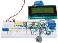
Some comments on the photo: The PIC is being programmed while on the
solderless breadboard by using the 6 Position 6 Contact RJ11 modular jack (Jameco 124038 or
124039: 1=wht=Vpp, 2=blk=+5, 3=Red=Gnd, 4=Grn=PGD, 5=Yel=PGC, 6=Blu=nc) by means of
the Microchip ICD 2. This particular jack comes with wires
already attached so you just plug them into the board and away you
go. I made up an adapter from a machined 16 pin DIP socket (note
that machined pin sockets will plug into solderless breadboards, but
the cheaper ones have short skinny legs and do not work) by soldering a
2x8 pin 0.1" header to the socket using short wires and hot melt
glue. This allows easy connection to a ribbon cable IDC attached
to any of a number of LCD modules. I still have not found a good
way to connect a ribbon cable to the 1x16 LCD module, the 2x7 or 2x8
LCD module connection is perfect for a ribbon cable. For
debugging I put an LED (+ 470 Ohm resistor) on each of the shift
register inputs and outputs. By using the LED blinking program
above to drive the clock line at about 1 pulse per second and manually
plugging the data line into +5 or ground it was easy to check it out
and get it going. Note that you can not manually plug the clock line
into +5 or ground and get only one transition, because of bounce you
get a large number of clocks.
Most
character LCD modules use a controller chip that's compatible with the
no longer made HD44780. It uses a data bus of either 8 or 4 bits
and in addition a control bus with Register Select (RS), Enable strobe
to start an action and a R/W pin to allow reading back the Busy Flag
(BF) or address or data from the module. So you need 11 (8 bit
mode) or 7 (4 bit mode) wires (I/O pins) to talk directly to the
module and use all it's features, or one
less if you only want to talk to it. But for a micro controller
that always seems to be short I/O pins (see above) this is way too many
pins.
You can buy new surplus LCD modules for between $1 and $5. The
ones with LED backlights are the easiest to activate. EL and CCFL back lights require HV AC supplies.
Photo above shows a working 2-wire interface based on Myke's design.
This uses a total of 2 I/O pins to talk only to the LCD module which is
running in 4 bit mode.
There are a number of alternative ways to control a character LCD module using a small number of pins.
- One way is to use one of the "Serial LCD" modules. These
typically have a PIC micro controller acting as a one way or two way serial
interface that usually can be used either with RS-232 levels and
inverted data or with TTL levels and normal data. Scott Edwards,
Matrix Orbital, Crystalfontz &c. are typical vendors of these $40
and up solutions. The PIC is smart and knows about the LCD
character position addressing.
- Scott Edwards -
Matrix Orbital -
Crystalfontz - LCDC (only for CF)
- Peter Anderson sells preprogrammed PICs ($5+) that do the same thing. A printed circuit board is available from Wulfden
for $4+. So with some more parts and your labor you have a serial
LCD. The PIC is smart and knows about the LCD character position
addressing.
- Myke 2-Wire LCD interface
- Using a pin for serial data and another for serial clock the bits for
D7, D6, D5, D4, RS, and E are clocked into a hex FF wired as a shift
register and with some cleverness control the LCD. The parts cost
is under $1, but the micro controller needs to do some bit
banging. I have this working as shown in the photo.
Although I don't have a Basic Stamp I would think this would work with
the stamp since slow timing would not be a problem. If you know
if it works or not let me know.
This
circuit might be improved by using the 8-bit 74HC595 shift
register instead of the original 6-Flip-Flop 74LS174. The idea
would be to use one of the new bits as the tri-state control of the
595. When the outputs were active the operation would be as
before. The other new bit can be connected to the R/W line on the
LCD. Now when 595 tri-state is active and R/W is set for Read the
LCD D7 pin has the Busy Flag (BF). This could be read using an
additional PIC pin. So now a simple 3-wire interface includes the
BF read back which may be a big help since the LCD instruction cycle
timing today varies all over the place because of the 3 volt vs. 5 volt
operation and controller chip clock resistor values. Also very
helpful for reading the cursor position and current data value when
doing LCD navigation.
Direct Parallel control of the lines with a PC can also be done.
Links
Back to Brooke's Products for Sale, Home, Electronics,
Computer, Precision
Clock page.
[an error occurred while processing this directive] time
this page created 20 Jan 2000.
 Some comments on the photo: The PIC is being programmed while on the
solderless breadboard by using the 6 Position 6 Contact RJ11 modular jack (Jameco 124038 or 124039: 1=wht=Vpp, 2=blk=+5, 3=Red=Gnd, 4=Grn=PGD, 5=Yel=PGC, 6=Blu=nc) by means of
the Microchip ICD 2. This particular jack comes with wires
already attached so you just plug them into the board and away you
go. I made up an adapter from a machined 16 pin DIP socket (note
that machined pin sockets will plug into solderless breadboards, but
the cheaper ones have short skinny legs and do not work) by soldering a
2x8 pin 0.1" header to the socket using short wires and hot melt
glue. This allows easy connection to a ribbon cable IDC attached
to any of a number of LCD modules. I still have not found a good
way to connect a ribbon cable to the 1x16 LCD module, the 2x7 or 2x8
LCD module connection is perfect for a ribbon cable. For
debugging I put an LED (+ 470 Ohm resistor) on each of the shift
register inputs and outputs. By using the LED blinking program
above to drive the clock line at about 1 pulse per second and manually
plugging the data line into +5 or ground it was easy to check it out
and get it going. Note that you can not manually plug the clock line
into +5 or ground and get only one transition, because of bounce you
get a large number of clocks.
Some comments on the photo: The PIC is being programmed while on the
solderless breadboard by using the 6 Position 6 Contact RJ11 modular jack (Jameco 124038 or 124039: 1=wht=Vpp, 2=blk=+5, 3=Red=Gnd, 4=Grn=PGD, 5=Yel=PGC, 6=Blu=nc) by means of
the Microchip ICD 2. This particular jack comes with wires
already attached so you just plug them into the board and away you
go. I made up an adapter from a machined 16 pin DIP socket (note
that machined pin sockets will plug into solderless breadboards, but
the cheaper ones have short skinny legs and do not work) by soldering a
2x8 pin 0.1" header to the socket using short wires and hot melt
glue. This allows easy connection to a ribbon cable IDC attached
to any of a number of LCD modules. I still have not found a good
way to connect a ribbon cable to the 1x16 LCD module, the 2x7 or 2x8
LCD module connection is perfect for a ribbon cable. For
debugging I put an LED (+ 470 Ohm resistor) on each of the shift
register inputs and outputs. By using the LED blinking program
above to drive the clock line at about 1 pulse per second and manually
plugging the data line into +5 or ground it was easy to check it out
and get it going. Note that you can not manually plug the clock line
into +5 or ground and get only one transition, because of bounce you
get a large number of clocks.